

Semiconductor Lithography Equipment Market: Growth, Trends, and Future Outlook
The semiconductor lithography equipment market plays a critical role in the global semiconductor manufacturing ecosystem. Lithography equipment is essential for transferring intricate circuit patterns onto semiconductor wafers, enabling the production of advanced integrated circuits. As the demand for smaller, faster, and more efficient electronic devices continues to grow, the importance of precision-driven lithography technologies is increasing significantly.
The market is experiencing steady growth due to the expansion of consumer electronics, data centers, automotive electronics, and emerging technologies such as artificial intelligence and 5G. Semiconductor manufacturers are investing heavily in advanced lithography equipment to enhance chip performance and reduce power consumption. Additionally, the transition toward smaller process nodes is further driving the demand for cutting-edge lithography systems.
Get Your Sample Report Here: https://straitsresearch.com/report/semiconductor-metrology-and-inspection-equipment-market/request-sample,
Market Size
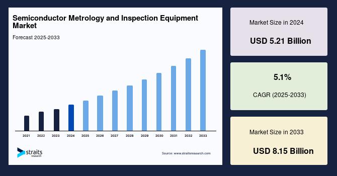
The global semiconductor metrology and inspection equipment market size was valued at USD 5.21 billion in 2024.
It is estimated to grow from USD 5.48 billion in 2025 to reach USD 8.15 billion by 2033, growing at a CAGR of 5.1% during the forecast period (2025-2033).
Market Overview
Semiconductor lithography equipment is used in the fabrication process to print patterns onto silicon wafers. This process is fundamental to the production of integrated circuits and microchips. The increasing complexity of semiconductor devices and the need for higher precision are driving advancements in lithography technologies.
The market is influenced by the growing demand for high-performance computing, smartphones, and connected devices. The shift toward extreme ultraviolet lithography is enabling the production of smaller and more powerful chips. Furthermore, the integration of advanced metrology and inspection equipment is improving manufacturing efficiency and yield rates.
Market Drivers
Rising Demand for Advanced Semiconductor Devices
The increasing demand for high-performance electronics, including smartphones, laptops, and IoT devices, is driving the need for advanced semiconductor manufacturing technologies.
Growth of Artificial Intelligence and Data Centers
AI applications and data centers require powerful processors, which in turn demand advanced lithography techniques for chip production.
Technological Advancements in Lithography
Innovations such as extreme ultraviolet lithography are enabling manufacturers to produce smaller and more efficient chips, supporting market growth.
Expansion of Automotive Electronics
The growing adoption of electric vehicles and autonomous driving technologies is increasing the demand for semiconductors, thereby boosting the lithography equipment market.
Market Challenges
High Capital Investment
Lithography equipment is expensive, requiring significant investment from semiconductor manufacturers, which can limit market growth.
Complexity of Technology
The development and operation of advanced lithography systems require highly specialized expertise and resources.
Supply Chain Constraints
The semiconductor industry faces supply chain challenges that can impact the availability of equipment and components.
Market Segmentation
By Equipment Type
Lithography Systems
Lithography systems are the core equipment used for patterning semiconductor wafers. These systems are continuously evolving to support smaller nodes and higher precision.
Metrology Equipment
Metrology equipment is used to measure and analyze wafer properties, ensuring accuracy in the manufacturing process.
Inspection Equipment
Inspection equipment helps identify defects in wafers, improving yield and reducing production costs.
By Technology
Deep Ultraviolet Lithography
Deep ultraviolet lithography is widely used in semiconductor manufacturing due to its reliability and cost-effectiveness.
Extreme Ultraviolet Lithography
Extreme ultraviolet lithography is an advanced technology that enables the production of smaller and more complex chips.
By Application
Integrated Device Manufacturers
These companies design and manufacture semiconductor devices, driving demand for lithography equipment.
Foundries
Foundries provide manufacturing services for semiconductor companies and are major users of lithography systems.
By End-User
Consumer Electronics
The consumer electronics segment dominates the market due to high demand for smartphones, tablets, and wearable devices.
Automotive
The automotive industry is increasingly adopting semiconductor technologies for advanced driver assistance systems and electric vehicles.
Telecommunications
Telecom applications require advanced semiconductors for 5G networks and communication infrastructure.
Industrial
Industrial applications include automation, robotics, and smart manufacturing systems.
Regional Analysis
North America holds a significant share of the semiconductor lithography equipment market due to the presence of leading semiconductor companies and advanced research facilities. Europe is also a key market, driven by technological innovation and strong industrial base.
Asia-Pacific dominates the global market and is expected to witness the fastest growth. The region is home to major semiconductor manufacturing hubs, including China, Taiwan, South Korea, and Japan. Increasing investments in semiconductor fabrication facilities are driving market growth in this region.
Top Players Analysis
- ASML Holding N.V.
ASML is a global leader in lithography equipment, known for its advanced extreme ultraviolet systems. - Nikon Corporation
Nikon provides high-performance lithography systems used in semiconductor manufacturing. - Canon Inc.
Canon offers a range of lithography equipment with a focus on precision and efficiency. - KLA Corporation
KLA specializes in metrology and inspection equipment, supporting semiconductor manufacturing processes. - Applied Materials Inc.
Applied Materials provides a wide range of semiconductor equipment, including solutions for lithography and inspection.
These companies are focusing on research and development, innovation, and strategic collaborations to maintain their competitive edge in the market.
Future Opportunities
The semiconductor lithography equipment market offers significant growth opportunities driven by technological advancements and increasing demand for advanced chips. The development of next-generation lithography technologies is expected to enable further miniaturization and performance improvements.
The growing adoption of artificial intelligence, Internet of Things, and 5G technologies is creating new opportunities for semiconductor manufacturers. Additionally, government initiatives to promote domestic semiconductor production are supporting market growth.
Emerging applications such as quantum computing and advanced packaging technologies are also expected to drive demand for lithography equipment in the future.
Conclusion
The semiconductor lithography equipment market is poised for steady growth, driven by increasing demand for advanced semiconductor devices and continuous technological innovation. Despite challenges such as high costs and complexity, the market offers substantial opportunities for growth and development. Key players are focusing on innovation and strategic initiatives to meet the evolving demands of the semiconductor industry.
Buy Now to Access Detailed Semiconductor Equipment Market Insights and Stay Ahead in the Competitive Landscape: https://straitsresearch.com/buy-now/semiconductor-metrology-and-inspection-equipment-market,
Frequently Asked Questions (F&Q)
What is semiconductor lithography equipment?
Semiconductor lithography equipment is used to transfer circuit patterns onto wafers during the chip manufacturing process.
What is driving the market growth?
The market is driven by the demand for advanced electronics, AI applications, and technological advancements in lithography.
Which segment dominates the market?
Consumer electronics is the leading segment due to high demand for electronic devices.
What are the major challenges?
High costs, technological complexity, and supply chain issues are key challenges.
What is the future outlook?
The market is expected to grow steadily with advancements in lithography technologies and increasing semiconductor demand.
About Us:
Straits Research is a market intelligence company providing global business information reports and services. Our exclusive blend of quantitative forecasting and trends analysis provides forward-looking insight for thousands of decision-makers. Straits Research Pvt. Ltd. provides actionable market research data, especially designed and presented for decision making and ROI.
Contact Us:
Email: sales@straitsresearch.com
Tel: +1 646 905 0080 (U.S.), +44 203 695 0070 (U.K.)